The guys at The Enquirer seem to have some dough about the next generation GPU from nVidia , In an analyst webcast, Nvidia Investor Relations and Communications VP Michael Hara stated the top end card based on the G92 graphics processor will be ready for Christmas and that it will have computing power close to 1 TeraFLOP .
Time for some cools stats now , Intel’s latest quad core Core 2 extreme QX6700 runs at 2.6 GHz and has a peak floating point performance of 50 GFLOPS, while nVidia’s G80 ( powers the 8800GTX) has a peak floating point performance of 330 GFLOPS, AMD’s R600 can do a max 450 GFLOPS and the STI Cell B.E does close to 250 GFLOPS at max throughput . So if the G92 rumor holds it would mean that the G92 will outperform the cell by around 4 times and its predecessor G80 by about 3 times in terms of computing power.
One problem with GPU’s is the inability to support 64 bit floating point operations, which is necessary for almost all supercomputing applications . On the other hand GPU’s are far cheaper than supercomputer vector processors making their use in HPC( High performance computing) justified . nVidia had promised FP64 support on GPUs by late 2007 , So is G92 the promised chip , if so its going to have a big impact on the GPGPU movement and on HPC in general.
One little concern for me is the lack of titles for the PC which can take advantage of such horsepower , Crysis is a contender and so is SC-Conviction . TeraFLOP or not it’ll be interesting to see what kind of performance can the G92 can dish out.
processors
May 25, 2007
May 24, 2007
Multi-core architectures – parting ways
Posted by Ashwin under processors, Tech watchLeave a Comment
From the recent announcements of the chip majors , it seems the catch up games that they have been playing with each other are over.
What am I talking about ? First it was all about pushing clock speeds up , and more recently it’s been about putting more cores on a chip more efficiently than the other . But as the multicore architectures become more mature , chip majors like Intel and AMD have started to diverge on their multicore strategies . Intel is moving towards homogeneous cores while AMD and IBM look to be adopting a more heterogeneous approach .
Homogeneous as the word implies means all the processing units (cores) on a certain processor are of the same type and divide the workload between them for maximum efficiency . The heterogeneous approach is a little more complicated as it may be implemented in a lot of ways , different size cores for different dedicated functions is one approach . Another approach is where a problem’s workload is split between a general-purpose processor and one or more specialized, problem-specific processors. Heterogeneous computing is a broader research area and the concept has been around for a while now, it also encompasses efforts like GPGPU computing , the Clearspeed accelerators and more recent efforts like the AGEIA PHYSX co processor .The most recent and the best example of a heterogeneous processor would be the STI Cell B.E with its Power PC core and the 8 synergistic processor units . AMD has plans for a similar architecture and their first heterogeneous multicore offering may be a CPU and GPU in the client space.
On the software side ,task-level parallelism and workload partitioning continue to be the dominant issues for multi-core platforms for both heterogeneous and homogeneous architectures. These issues will be more acute on heterogeneous multi-core systems, since the specialized processors will throw up a new set of problems. I believe heterogeneous computing is geared towards extreme performance computing , the GPGPU movement and the Cell’s performance with folding@home proves this point. General purpose computing might go the homogeneous way , as the challenges are far lesser and are fast being resolved .
April 30, 2007
The Future of Processing – Multicore and Beyond
Posted by Ashwin under processors, Tech watch[4] Comments

Computing has come a long way , remember the cray-1, it could do one Gigaflop . Recently AMD announced Teraflop in a box : One Opteron processor and two R600 Gpu’s combining to dish out more than 1 trillion floating-point calculations per second using a general “multiply-add” calculation . Intel at their Beijing IDF showed off their concept 80 core teraflop processor . The Cell B.E is a multicore processor of sorts with one PPE and eight SPE’s capable of crunching out 256Gflops . Teraflop scale processing is already happening on the cell with folding@home and the PS3 and according to reports its showing some great results.
With the industry moving towards this parallel processing revolution , the development on the software side of things seems to be remarkably slow , What I mean here is that the software which uses these multicore processors should be optimized for the same , Most of the ISV’s don’t have in-house programming expertize to do multithreading applications.Switching from one core to many core presents its own set of developmental , and debugging challenges and a large percentage of mission-critical enterprise applications are not “multi-core optimized ” leading to applications not showing any kind of performance boost when switched to multicore processors and in some cases showing even poorer performance, this happens because a single-threaded application can’t utilize the additional cores in the processor efficiently without sacrificing ordered processing. This results in a huge drop in performance due to cores being not optimally utilized . Currently there are no automated compilers for multicore processors , then there is the problem of application priority, there are many such issues which need to be sorted out before the transition to multicore can be complete.
Moving further,The Cell B.E is going mainstream slowly with IBM announcing a new line of servers powered by the Cell B.E . Researchers have already released initial details about the EDGE processor architecture , which stands for Explicit Data Graph Execution.Instead of one instruction at a time, EDGE handles large blocks of data all at once. Using many copies of a small number of replicated tiles, the target for TRIPS ( the first prototype chip on the EDGE architecture ) by 2009 is to hit 5 TFLOPs on 32nm manufacturing. Intel is also looking at Larabee to give them similar numbers.
In the future , there is a good chance that we will be moving to some non X-86 ISA processor , which does the job in a better more efficient way.
More on EDGE and TRIPS
A whitepaper on EDGE
April 24, 2007
AMD celebrates AMD64 Anniversary with a new Opteron and Barcelona
Posted by Ashwin under hardware, processors, Tech watch1 Comment
![]()
April 23rd marked the fourth anniversary for the chipmaker’s Opteron and the ground-breaking AMD64 architecture , and to mark the occasion AMD announced widespread availability and pricing for the latest range of AMD Opteron dual-core server processors .
AMD also revealed updated performance numbers for its upcoming Quad-Core AMD Opteron™ processors, code-named ‘Barcelona.’ The new Barcelona projections show that AMD expects to have up to a 50 percent advantage in floating point performance and 20 percent in integer performance over the Intel’s “clovertown” quad-core processor at any given common clock frequency.AMD did not specify the clock speed of Barcelona. Intel’s Clovertown currently tops the chart at 2.66 GHz.
As for the performance of the new AMD Opteron Model 2222 and 8222 SE x86 dual-core server processors . AMD claims and I quote their website
“Under the newest SPECcpu2006 benchmarks, AMD Opteron™ processors continue to set the standard in x86 dual-core processor performance—besting our competitor by up to 15%. We credit that to our superior native dual-core design, with its Direct Connect Architecture, DDR2 memory, and industry-leading performance-per-watt. All with a clear migration path to native Quad-Core. It’s all proof positive that customer-centric innovation wins over hype.”
The AMD site also says
“Saying you’re the “World’s Best Processor” is one thing.
Actually being the “World’s Best Processor” is another.”
Considering their Dismal Q1 results , I would consider it a bold statement
More performance numbers
AMD Native Quad Core Tchnology
See the video where Randy Allen, Corporate Vice-President of AMD’s Server and Workstation Business talks about Barcelona
April 23, 2007
Silicon Stacking – Packaging solution for the future
Posted by Ashwin under hardware, Memory, processors[2] Comments

The demand for smaller-sized, high-speed, high-density multi-chip packages (MCP) is growing by the day . Stacking Silicon to increase packing density in IC’s is not a new concept, but recently stacking has gained a new level of importance as the process is being introduced to make microprocessors and is slated to come into the mainstream by 2008,Currently chip components are connected by wire bonding, requiring vertical spacing between dies that is tens of microns deep and horizontal spacing on the package board hundreds of microns wide for the die-connecting wires.Stacked silicon, rather than placed side-by-side shortens on chip data travel distances, ultimately saving a whole lot of space on chip and offering an opportunity to drive Moore’s law forward .
“Through-silicon vias” (TSV) is the technology employed for stacking ,which uses vertical connections etched through the silicon wafer and filled with metal. This concept has been described by other chip manufacturers before . Intel revealed thier plans for TSV at the spring IDF 2005 and most recently Samsung announced that it has developed the first all-DRAM stacked memory package using TSV technology, which will soon result in memory packages that are faster, smaller and consume less power, Samsung’s technology forms laser-cut micron-sized holes that penetrate the silicon vertically to connect the memory circuits directly with a copper filling, eliminating the need for gaps of extra space and wires protruding beyond the sides of the dies.
While TSV is still in its early stages, the technology represents the next step in innovative packaging solutions which have become increasingly important to enable high-speed, high-density and high- performance Semiconductor solutions .
April 20, 2007
Pico-ITX A mainboard to fit you pocket
Posted by Ashwin under hardware, Mainboard, processors, Tech watch[2] Comments
![]()
Via Technologies , the Taiwanese manufacturer of Integrated circuits who also happen to be the world’s largest independent manufacturer of motherboard chipsets , have announced the IT industry’s smallest mainboard form factor specification and they call it Pico-ITX , at 10cm x 7.2cm it measures in slightly bigger than a regular playing card , Pico-ITX is currently the smallest complete x86 mainboard in the industry, smaller than all existing ATX, BTX and ITX form factors.


Designed for the Via range of processors such as the C7 processor , Pico-ITX mainboard form factor will provide system developers and with a standardized, ultra compact and highly integrated platform that can be utilized across multiple embedded PC, system and appliance designs. Some examples where these can be used may be PCs embedded within dashboards or in-flight entertainment systems and industrial automation systems , Integrated multimedia devices and even ultra portable entertainment devices, Pico-ITX can enable the design of full x86 computing devices in form factors which were previously not practical due to size limitations. Though I don’t see the design being utilized to its full potential in the very near future but come 2008 one can expect a lot of movement in the UMPC sector . The reference design specification has the following key components
Processor :VIA C7/VIA Eden V4 bus processor
•NanoBGA2 package up to 1.5GHz
• 128K L1 and 128K L2 cache
Core Logic: VIA VX700 all-in-one system media processor
Main Memory : • 1 DDR2 400/533 So-DIMM socket
• Up to 1GB memory size
Graphics: • Integrated VIA UniChrome™ Pro II 3D/2D AGP graphics with MPEG-2/4 and WMV9 video decoder
• Integrated LVDS and DVI interface • VIP port for video overlay function
Storage (ATA) • UltraDMA 133/100/66/33
• One 44-pin right-angle IDE connector
• One SATA connector
Audio System: VIA VT1708A
• 7.1 channels high definition audio codec
• 7.1 channels audio out and SPDIF in header
• Sound Blaster, Sound Blaster Pro compatible
Ethernet: (LAN) VIA VT6106S
• 10/100Mbps Ethernet Controller
April 17, 2007
Intel Penryn – first performance numbers Revealed
Posted by Ashwin under hardware, processors, Tech watch[2] Comments
![]()
Intel has revealed the first performance numbers for their upcoming 45nm Penryn Series of processors at their spring IDF in Beijing . Penryn will make its debut in late 2007 or early 2008 and is the successor to the current line up of Core 2 Duo processors made on the 65nm process.
Intel gave out performance numbers of the new processor with a comparison to its current top of the line 2.93 GHz Kentsfield QX6800 CPU . In comparison the new 3.33 GHz Yorkfield processor (Penryn quad-core for desktops) with 12 MB L2 cache and FSB1333 will gain about 15% in imaging applications, 25% for 3-D Rendering, 40% or more for gaming and more than 40% faster video encoding with SSE4 optimized video encoders, This performance gain comes from the fact that Intel has a set of 47 new SSE instructions to enhance the performance of such CPU intensive Applications .
On the server and workstation side, Intel expects its 45 nm FSB1600 processors to deliver up to 45% more speed for Bandwidth Hungry applications and a 25% acceleration for servers which use Java, when compared to the current X5355 quad-core processor.
Intel also intends to announce Skulltrail : a Consumer dual socket solution for Penryn which would allow up-to 8 cores on two chips and 4 graphics card on board , It should be noted that AMD has such a platform out for some time now which I had written about ( Quad Fx) . For more information on Penryn visit the IDF site ,The session Files can be downloaded in the PDF format.
January 4, 2007
Intel – Driving Moore’s law forward with 45nm Manufacturing
Posted by Ashwin under processors, Tech watchLeave a Comment
![]()
The first Pentium processor’s spec sheet looked like this

| Core Frequency: | 75 MHz |
| Board Frequency: | 50 MHz |
| Clock Multiplier: | 1.5 |
| Data bus (ext.): | 64 Bit |
| Address bus: | 32 Bit |
| Transistors: | 3,300,000 |
| Circuit Size: | 0.60 µ |
| Voltage: | 3.3 V |
The Pentium series was largely fabricated on the then cutting edge 350nm technology, silicon fabrication technology has come a long way since then, the latest Core 2 Duo line of Intel Microprocessors are fabricated on the 65nm process and have more than 150 times the number of transistors than the first Pentium chip. Intel has produced the first ever fully functional SRAM chip based on the 45nm process technology, and is on track to start large scale manufacture by 2nd half of 2007.
Increasing transistor density and decreasing the amount of power used are the two greatest challenges which drive Silicon technology today , 45nm chips will have a greater performance/Watt advantage and will enable engineers to squeeze in twice the number of transistors in the same given area, this will enable smaller chip sizes and more number of transistors per chip which are very important for mobile devices . The new technology also promises a significant increase in transistor switching speeds and decreased transistor leakage which will eventually lead to smaller low power – high performance devices. TI has also made remarkable progress on this front and they plan to use their 45nm process to make memory chips, while we’ll have to wait a little longer before AMD announces their 45nm process .
December 28, 2006
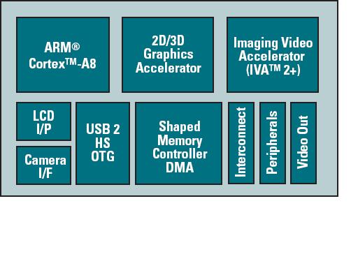
TI OMAP 3430 Multimedia applications processor
Posted by Ashwin under processors, Tech watch[4] Comments

“wireless handheld communication Device” – sound familiar, commonly known as the cell phone for many is just a magical piece of hardware which can do just about anything , make phone calls , access e-mails ,take pictures , play games and the list goes on and on . well it just got better . TI’s OMAP 3 architecture and the first offering named the OMAP3430 promises to revolutionize mobile multimedia.
designed to deliver laptop like performance, 3430 is also the industry’s first applications processor to be designed using the 65nm manufacturing technique, has the highest clock speed and marks huge advancements over the company’s OMAP 2 series .
The chip is based aorund the ARM Cortex A8 processor and also inclutes an integrated 2D/3D graphics processor, TI estimates that one can expect up to 4X performance increase in multimedia applications which means better audio and video playback , better games and a smoother interface, the integrated graphics processor also enables multiple formats like Real video , windows media video and mpeg , mpeg-4 etc, it features an on chip camera image pipeline which removes the need for external circuitry i.e camera phones based on it won’t weigh a ton, camera sensors up to 12 Mega-pixels are supported by the chip, the 3430 also features extended output capabilities , it can connect directly to VGA and S-Video outputs without needing any external interface , it even has fully compliant HDD interfaces and USB2.0 interface and also compliant with all the High level operating systems like Linux , Windows mobile and Symbian
a very high level architecture diagram is given below , more information can be found at the TI OMAP website